Executive Overview: A Paradigm Shift in Semiconductor Supremacy
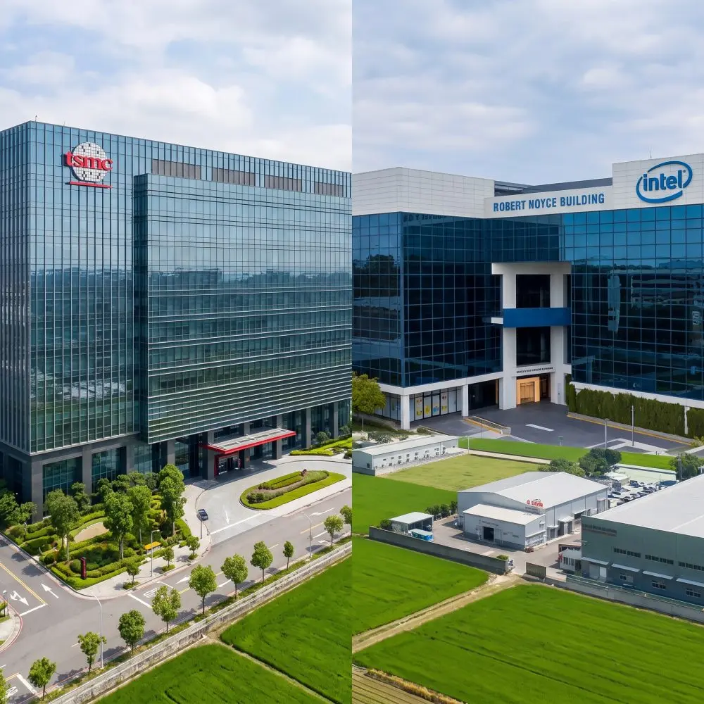
Currently, the global AI infrastructure relies almost exclusively on Taiwan Semiconductor Manufacturing Company’s (TSMC) CoWoS (Chip-on-Wafer-on-Substrate) technology. This process allows for the integration of massive AI accelerators with High-Bandwidth Memory (HBM) on a single, high-performance package. Yet, this dominance has created a global supply chain bottleneck. As lead times for Nvidia’s H100 and Blackwell GPUs remain extended, industry analysts are pointing toward a significant vulnerability in TSMC’s armor.
According to Neil Shah, co-founder of Counterpoint Research, and other leading industry voices, the high costs, yield risks, and capacity constraints associated with TSMC’s CoWoS are creating a "credible opening" for Intel Foundry. By leveraging its proprietary EMIB (Embedded Multi-die Interconnect Bridge) and Foveros 3D stacking technologies, Intel is positioning itself not just as a domestic alternative to TSMC, but as a technically superior partner for the next generation of AI silicon. This report explores the technical, economic, and geopolitical factors driving this potential migration of "Big Tech" silicon toward Intel’s fabrication plants.
Detailed Chronology: The Road to the Packaging Bottleneck
2021–2023: The CoWoS Ascendancy
During the initial explosion of Large Language Models (LLMs), TSMC’s CoWoS became the industry standard. Companies like Nvidia, AMD, and Broadcom utilized CoWoS-S (using silicon interposers) to connect compute dies with HBM. While effective, the process is inherently "thick" and expensive, requiring a large silicon interposer that acts as a bridge between the chiplets.

Late 2023: The Capacity Crisis
By the end of 2023, it became clear that TSMC could not scale CoWoS capacity fast enough to meet the insatiable demand for AI chips. This scarcity led to a "waitlist" for AI accelerators, prompting cloud service providers (CSPs) like Google and Amazon to accelerate their in-house ASIC (Application-Specific Integrated Circuit) programs.
Early 2024: Intel’s Strategic Pivot
Intel, under the leadership of CEO Pat Gelsinger, accelerated the separation of its design and foundry businesses. By proving the viability of EMIB in high-volume products like Sapphire Rapids, Intel demonstrated that it could integrate multiple dies without the need for the massive, yield-killing silicon interposers used by TSMC.
August 2024: The Counterpoint Revelation
A report from Counterpoint Research, highlighted by EE Times, officially identified TSMC’s interposer reliance as a "steep cost" barrier. The report suggests that major players—most notably Google and MediaTek—are already looking toward Intel’s EMIB-T for future Tensor Processing Units (TPUs), marking the first major defection from the TSMC ecosystem for high-end AI silicon.
Supporting Context & Metrics: The Technical Divide
The Interposer Problem: Yield vs. Cost
The primary critique of TSMC’s current methodology lies in the "scrap cost." In a CoWoS-S package, a large silicon interposer sits beneath the GPU and the HBM stacks.

- The Risk: If a defect occurs in the interposer or the interconnect during the final stages of assembly, the entire package—including thousands of dollars worth of GPU silicon and eight or more HBM stacks—must be scrapped.
- The Intel Alternative: Intel’s EMIB technology uses a small silicon "bridge" embedded directly into the organic substrate. This eliminates the need for a giant, expensive interposer, significantly reducing the surface area prone to defects and lowering the overall cost of the package.
Comparison of Advanced Packaging Architectures
| Feature | TSMC CoWoS-S | Intel EMIB |
|---|---|---|
| Interconnect Type | Large Silicon Interposer | Embedded Silicon Bridge |
| Scrap Risk | High (Loss of entire assembly) | Lower (Localized bridge) |
| Yield Sensitivity | High (Die-size limited) | Moderate |
| Primary Customers | Nvidia, AMD | Google (Rumored), Cisco |
| Scalability | Limited by Interposer Reticle | High (Modular bridges) |
Geopolitical Reinforcements
The shift isn’t merely technical; it is heavily influenced by American industrial policy. The recent revelation that the Trump administration took a 10% stake in Intel underscores the "national champion" status the company now holds. Furthermore, reports from the Wall Street Journal suggest that Apple—TSMC’s largest customer—is in preliminary talks to shift some chip production to Intel. This move is seen as a strategic hedge against regional instability in the Taiwan Strait and a response to U.S. government incentives to "re-shore" critical semiconductor manufacturing.
Official Statements: Industry Voices on the Transition
The consensus among analysts suggests that while TSMC remains the "safe" choice, the tide is turning.
Neil Shah, Co-founder of Counterpoint Research:
"HBM’s reliance on TSMC’s CoWoS silicon interposers carries steep costs with thick packages, yield risk, capacity constraints and high scrap costs, thus creating an opening for credible alternatives. Scrapping an assembled package because of an interconnect or interposer defect destroys thousands of dollars in silicon at the final step."
Handel Jones, CEO of International Business Strategies (IBS):
"Intel already has a number of important external customers for packaging with good growth potential over the next few years. Intel has good technology in packaging and is expanding capacity including in Santa Fe, New Mexico. From a performance and power-consumption perspective, enhancements in packaging tech will be more important than the migration from 2.0-nm to 1.4-nm chip processes."

Mike Demler, Independent Analyst:
"EMIB eliminates the interposer, and Foveros offers die-stacking and other features TSMC doesn’t have. If nothing else, Intel has an opportunity to pick up customers because of TSMC’s capacity shortage."
Lip-Bu Tan, Former Intel Board Member and Industry Veteran:
Tan has recently telegraphed the increasing importance of memory integration, signaling that Intel’s future lies in its ability to solve the "memory wall" that currently limits AI performance.
Future Outlook: Beyond the Interposer
As the industry looks toward 2026 and beyond, the competition will move into the "interposer-less" era. Intel is already preparing its next-generation solutions:
1. Z-Angle Memory (ZAM)
Developed in collaboration with Saimemory (a SoftBank subsidiary), ZAM is a stacked DRAM technology designed to be an energy-efficient alternative to HBM. By reducing the power required to move data between the compute die and memory, ZAM could provide Intel with a unique selling point for mobile AI and edge computing.

2. Cross-Batch Memory (XBM)
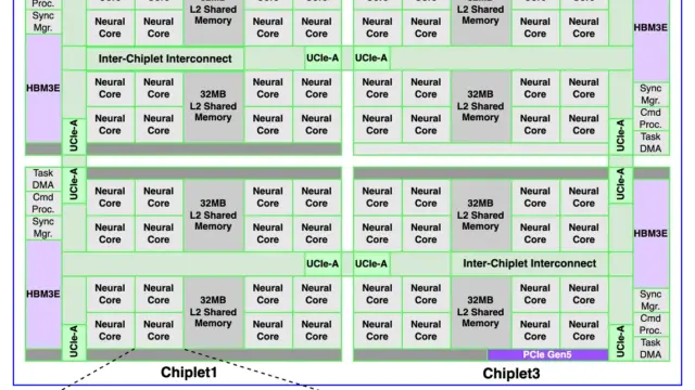
In the longer term, Intel aims to deploy XBM, which utilizes back-end-of-line (BEOL) thin-film transistors and serial UCIe (Universal Chiplet Interconnect Express) links. This would effectively eliminate the need for silicon interposers entirely, allowing for even denser and more cost-effective AI accelerators.
3. The 1.4-nm Frontier
While packaging is the current bottleneck, the race to the 1.4-nm node remains critical. Intel’s "14A" process is designed to work in tandem with Foveros Direct, allowing for copper-to-copper bonding that provides significantly higher interconnect density than TSMC’s current offerings.
Conclusion: A New Competitive Equilibrium
TSMC is not standing still; its CoWoS-L (Local Silicon Interconnect) is a direct response to Intel’s EMIB, utilizing localized bridges to improve yields. However, Intel’s advantage lies in its integrated model. By offering both the leading-edge nodes (18A/14A) and a more cost-effective, "bridge-based" packaging solution, Intel Foundry is positioned to break the TSMC monopoly.
The upcoming "Humufish" and "Triggerfish" TPUs from Google and MediaTek will serve as the first major litmus test. If Intel can execute these high-stakes designs with high yields and on-time delivery, it will signal the beginning of a new era in semiconductor manufacturing—one where the "Intel Inside" logo refers not just to the CPU, but to the very foundation of the AI revolution.